- 您现在的位置:买卖IC网 > Sheet目录3881 > PIC18F4539T-E/ML (Microchip Technology)IC PIC MCU FLASH 12KX16 44QFN
PIC18FXX39
DS30485A-page 264
Preliminary
2002 Microchip Technology Inc.
23.2
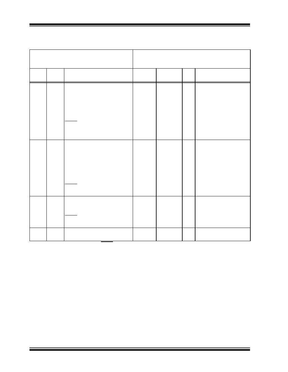
DC Characteristics: PIC18FXX39 (Industrial, Extended)
PIC18LFXX39 (Industrial)
DC CHARACTERISTICS
Standard Operating Conditions (unless otherwise stated)
Operating temperature -40°C
≤ TA ≤ +85°C for industrial
-40°C
≤ TA ≤ +125°C for extended
Param
No.
Symbol
Characteristic
Min
Max
Units
Conditions
VIL
Input Low Voltage
I/O ports:
D030
with TTL buffer
Vss
0.15 VDD
VVDD < 4.5V
D030A
—
0.8
V
4.5V
≤ VDD ≤ 5.5V
D031
with Schmitt Trigger buffer
RC3 and RC4
Vss
0.2 VDD
0.3 VDD
V
D032
MCLR
VSS
0.2 VDD
V
D032A
OSC1 (HS mode)
VSS
0.3 VDD
V
D033
OSC1 (EC mode)
VSS
0.2 VDD
V
VIH
Input High Voltage
I/O ports:
D040
with TTL buffer
0.25 VDD +
0.8V
VDD
VVDD < 4.5V
D040A
2.0
VDD
V4.5V
≤ VDD ≤ 5.5V
D041
with Schmitt Trigger buffer
RC3 and RC4
0.8 VDD
0.7 VDD
VDD
V
D042
MCLR, OSC1 (EC mode)
0.8 VDD
VDD
V
D042A
OSC1 (HS mode)
0.7 VDD
VDD
V
IIL
Input Leakage Current(1,2)
D060
I/O ports
.02
±1
AVSS ≤ VPIN ≤ VDD,
Pin at hi-impedance
D061
MCLR
—
±1
AVss ≤ VPIN ≤ VDD
D063
OSC1
—
±1
AVss ≤ VPIN ≤ VDD
IPU
Weak Pull-up Current
D070
IPURB
PORTB weak pull-up current
50
450
AVDD = 5V, VPIN = VSS
Note 1: The leakage current on the MCLR pin is strongly dependent on the applied voltage level. The specified
levels represent normal operating conditions. Higher leakage current may be measured at different input
voltages.
2: Negative current is defined as current sourced by the pin.
3: Parameter is characterized but not tested.
发布紧急采购,3分钟左右您将得到回复。
相关PDF资料
PIC18LF8680T-I/PT
IC PIC MCU FLASH 32KX16 80TQFP
PIC16F1936-I/SO
IC PIC MCU FLASH 512KX14 28-SOIC
PIC18F24K20-I/SO
IC PIC MCU FLASH 8KX16 28SOIC
PIC18LF8585T-I/PT
IC PIC MCU FLASH 24KX16 80TQFP
XF2J-3024-11
CONN FPC 30POS 0.5MM SMT
PIC18LF6525T-I/PT
IC PIC MCU FLASH 24KX16 64TQFP
PIC18LF8621T-I/PT
IC PIC MCU FLASH 32KX16 80TQFP
PIC18F8620T-E/PT
IC PIC MCU FLASH 32KX16 80TQFP
相关代理商/技术参数
PIC18F4539T-E/PT
功能描述:8位微控制器 -MCU 24KB 1408 RAM 32 I/O RoHS:否 制造商:Silicon Labs 核心:8051 处理器系列:C8051F39x 数据总线宽度:8 bit 最大时钟频率:50 MHz 程序存储器大小:16 KB 数据 RAM 大小:1 KB 片上 ADC:Yes 工作电源电压:1.8 V to 3.6 V 工作温度范围:- 40 C to + 105 C 封装 / 箱体:QFN-20 安装风格:SMD/SMT
PIC18F4539T-I/ML
功能描述:8位微控制器 -MCU 24KB 1408 RAM 32 I/O RoHS:否 制造商:Silicon Labs 核心:8051 处理器系列:C8051F39x 数据总线宽度:8 bit 最大时钟频率:50 MHz 程序存储器大小:16 KB 数据 RAM 大小:1 KB 片上 ADC:Yes 工作电源电压:1.8 V to 3.6 V 工作温度范围:- 40 C to + 105 C 封装 / 箱体:QFN-20 安装风格:SMD/SMT
PIC18F4539T-I/PT
功能描述:8位微控制器 -MCU 24KB 1408 RAM 32 I/O RoHS:否 制造商:Silicon Labs 核心:8051 处理器系列:C8051F39x 数据总线宽度:8 bit 最大时钟频率:50 MHz 程序存储器大小:16 KB 数据 RAM 大小:1 KB 片上 ADC:Yes 工作电源电压:1.8 V to 3.6 V 工作温度范围:- 40 C to + 105 C 封装 / 箱体:QFN-20 安装风格:SMD/SMT
PIC18F4550EPT
制造商:Microchip Technology Inc 功能描述:
PIC18F4550-I/ML
功能描述:8位微控制器 -MCU 32kBF 2048RM FSUSB2 RoHS:否 制造商:Silicon Labs 核心:8051 处理器系列:C8051F39x 数据总线宽度:8 bit 最大时钟频率:50 MHz 程序存储器大小:16 KB 数据 RAM 大小:1 KB 片上 ADC:Yes 工作电源电压:1.8 V to 3.6 V 工作温度范围:- 40 C to + 105 C 封装 / 箱体:QFN-20 安装风格:SMD/SMT
PIC18F4550-I/P
功能描述:8位微控制器 -MCU 32kBF 2048RM FSUSB2 RoHS:否 制造商:Silicon Labs 核心:8051 处理器系列:C8051F39x 数据总线宽度:8 bit 最大时钟频率:50 MHz 程序存储器大小:16 KB 数据 RAM 大小:1 KB 片上 ADC:Yes 工作电源电压:1.8 V to 3.6 V 工作温度范围:- 40 C to + 105 C 封装 / 箱体:QFN-20 安装风格:SMD/SMT
PIC18F4550-I/PT
功能描述:8位微控制器 -MCU 32kBF 2048RM FSUSB2 RoHS:否 制造商:Silicon Labs 核心:8051 处理器系列:C8051F39x 数据总线宽度:8 bit 最大时钟频率:50 MHz 程序存储器大小:16 KB 数据 RAM 大小:1 KB 片上 ADC:Yes 工作电源电压:1.8 V to 3.6 V 工作温度范围:- 40 C to + 105 C 封装 / 箱体:QFN-20 安装风格:SMD/SMT
PIC18F4550T-I/ML
功能描述:8位微控制器 -MCU 32kBF 2048RM FSUSB2 RoHS:否 制造商:Silicon Labs 核心:8051 处理器系列:C8051F39x 数据总线宽度:8 bit 最大时钟频率:50 MHz 程序存储器大小:16 KB 数据 RAM 大小:1 KB 片上 ADC:Yes 工作电源电压:1.8 V to 3.6 V 工作温度范围:- 40 C to + 105 C 封装 / 箱体:QFN-20 安装风格:SMD/SMT